In the race for artificial intelligence, we often hear about the power of GPUs or the number of parameters in large language models. But did you know that the printed circuit board (PCB)—the physical backbone connecting the entire system—is also facing unprecedented challenges?
The Race for Speed in Interconnect Standards
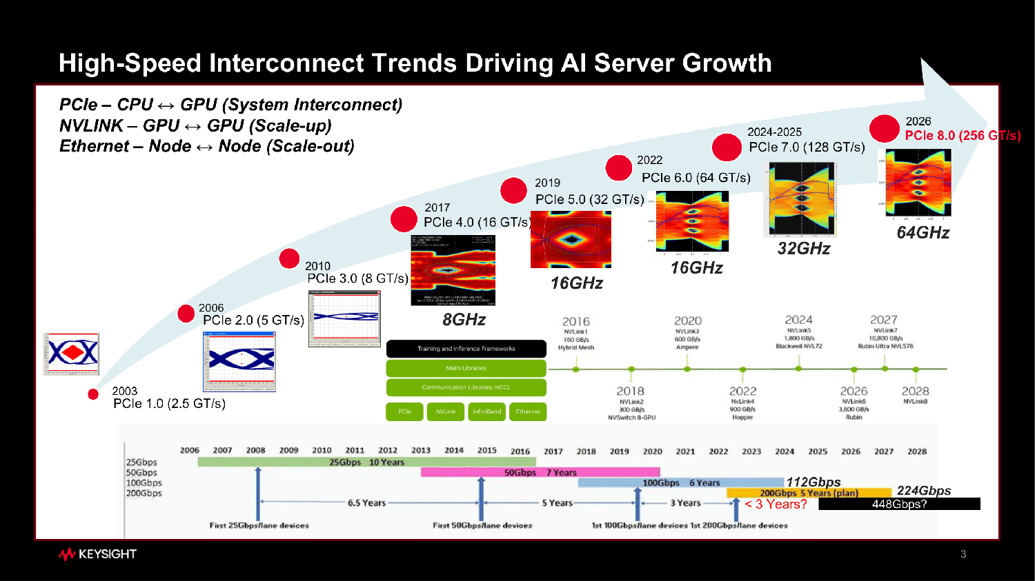
To better understand this, let’s look at the rapid leap in data speeds in recent years.
From PCIe 1.0 (2.5 GT/s) in 2003, we are now moving toward PCIe 7.0 (128 GT/s) and even PCIe 8.0 (256 GT/s) by 2026.
Operating frequencies have surged from 8 GHz to 64 GHz and beyond.
At these speeds, every trace on a PCB is no longer just a conductor—it becomes a highly sensitive transmission line.
The Shift in Priority: From Connectivity to Signal Integrity
As frequencies reach the GHz range, designers face an entirely new challenge—not just making connections, but preserving signal integrity.
In the past, PCB routing focused mainly on neat and efficient layouts. But in the AI era, long differential pairs have become the critical bottleneck—the most challenging aspect of PCB design.
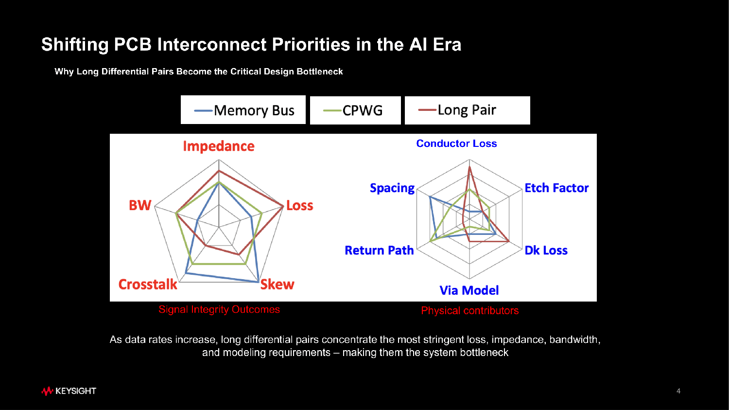
Looking at the chart on the left, you can see the negative “symptoms” affecting the signal: | This chart highlights the “root causes” behind the issues shown in the left-hand chart: |
Loss: Over long traces, signals weaken significantly from source to destination Skew: Signals in a differential pair do not arrive simultaneously; even small length mismatches can cause major errors Bandwidth limitations: AI demands ultra-high speeds, but long traces restrict bandwidth performance | Conductor Loss & Dielectric (Dk) Loss: Signal energy is lost due to copper and PCB substrate materials. The longer the trace, the greater the loss Via Model Effects: Vias (layer transitions) introduce signal discontinuities and distortion Etch Factor: Manufacturing inaccuracies during copper etching affect trace geometry |
The “symptoms” and “root causes” above lead us to an important question…
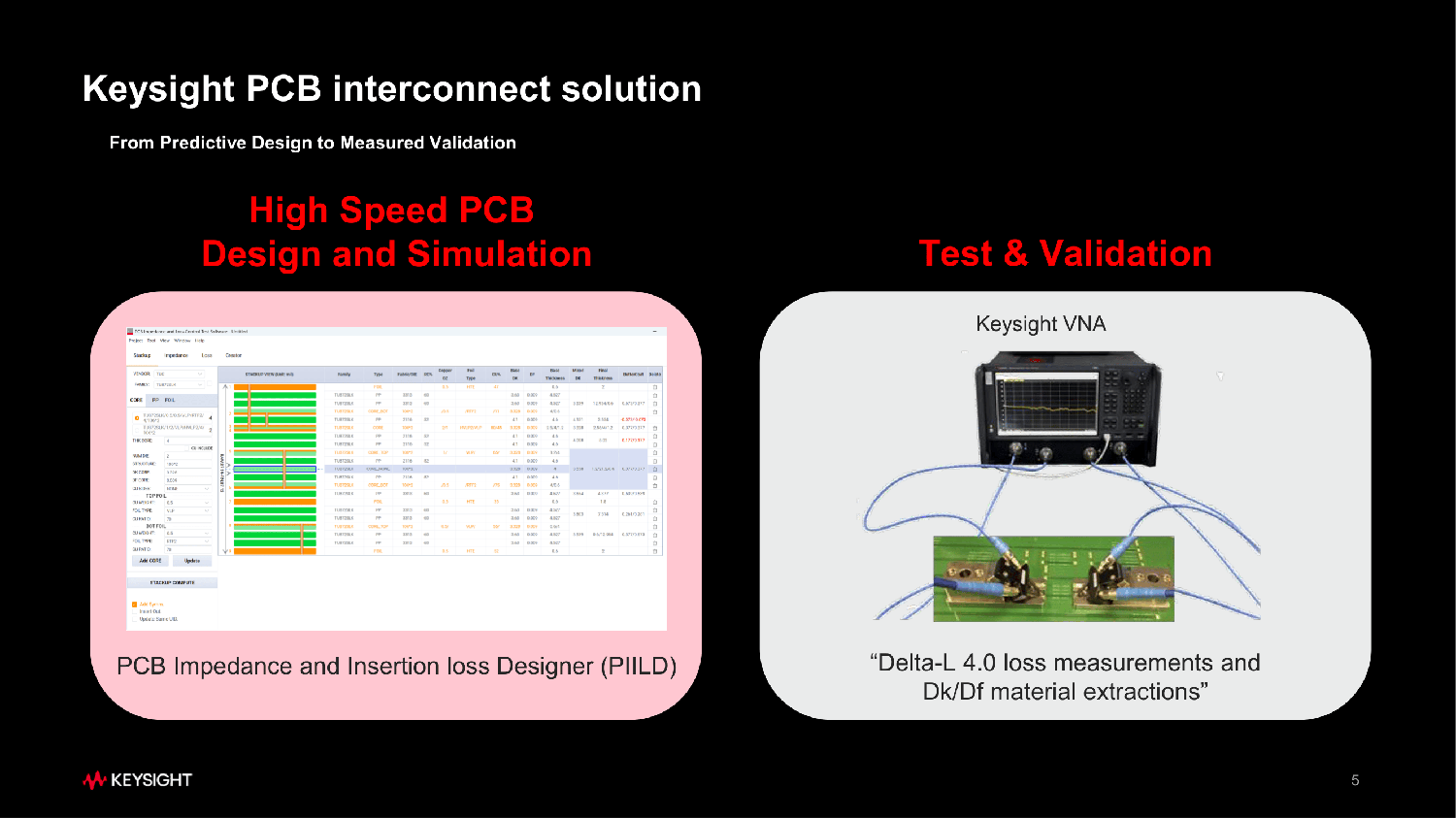
How can we ensure that a PCB design simulated on a computer will perform correctly in real-world conditions?
The answer lies in combining:
Simulation: Using electromagnetic (EM) solvers to predict material effects (Dk/Df)
Measurement: Using advanced instruments such as VNA and TDR, along with methods like Delta-L, to isolate losses and refine models.
Understanding the theory is one thing—but how can these processes be effectively applied in manufacturing to optimize cost and performance?
Join us to explore the answers at the technical seminar: “Enhancing Manufacturing Efficiency for Next-Generation Electronic Components and PCBs”
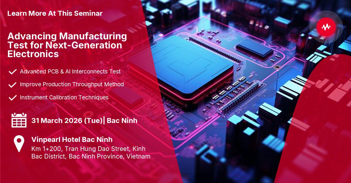
Location: Vinpearl Hotel Bac Ninh
Time: 13:30 – 17:15, Tuesday, March 31
These challenges are not just obstacles—they are opportunities for individuals and businesses ready to embrace cutting-edge technology. Don’t let your PCB infrastructure become the bottleneck of your AI system!