As we enter the 2026–2030 period, wide-bandgap (WBG) semiconductor materials such as Silicon Carbide (SiC) and Gallium Nitride (GaN) are transforming the power electronics, electric vehicle (EV/HEV), renewable energy, and AI data center industries. The shift from traditional silicon to SiC and GaN enables higher power density, smaller passive components, and improved overall system energy efficiency.
What Is Silicon Carbide?
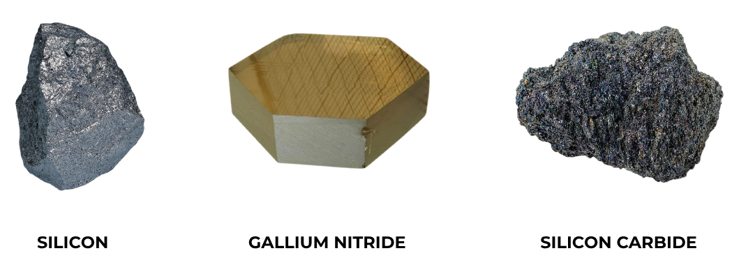
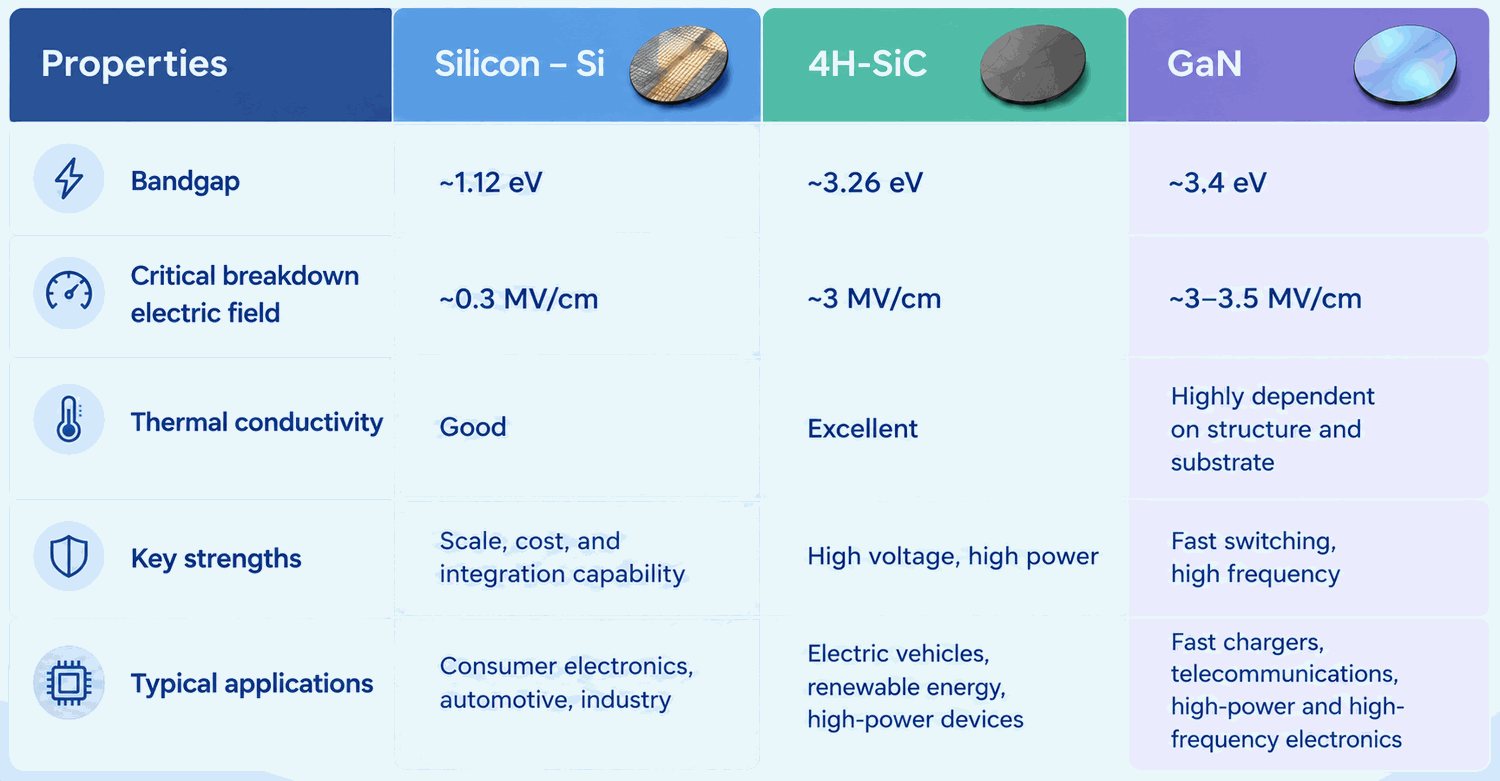
SiC (Silicon Carbide) is a third-generation semiconductor material belonging to the wide-bandgap semiconductor family. The bandgap is the minimum energy required for an electron to transition from the valence band to the conduction band, enabling electrical conduction. Although more energy is required to initiate conduction, this property offers significant advantages in power electronics. Compared with silicon devices of the same size, SiC-based components can withstand higher voltages, operate at higher temperatures, and support much higher switching frequencies without electrical breakdown or significant performance degradation.
Its outstanding physical properties include a Mohs hardness of 9–9.5, making it one of the hardest known materials, surpassed only by diamond and boron nitride. SiC also offers excellent thermal conductivity, outperforming copper under certain conditions, and maintains its strength at extremely high temperatures.
These properties have led to a wide range of Silicon Carbide applications. In industrial settings, SiC is used in abrasives, refractory materials for furnaces, and ceramic armor.
In semiconductor technology, Silicon Carbide enables the development of smaller, faster, and more efficient devices, including electric vehicle traction inverters and high-power DC fast-charging stations.
Comparing Si, SiC, and GaN
Although SiC is a prominent wide-bandgap semiconductor material, each semiconductor technology has its own advantages depending on the specific application. Therefore, silicon, SiC, and GaN are not universally interchangeable.
Failure Analysis Workflow for WBG Semiconductor Devices
Identifying failure mechanisms in SiC and GaN devices requires measurement and test systems with high bandwidth, low distortion, and excellent high-voltage isolation capabilities. Common failure modes include localized overheating that leads to die breakdown, gate oxide degradation in SiC MOSFETs caused by high electric fields, and charge trapping in GaN HEMTs, which can cause dynamic on-resistance to increase over time.
To address these challenges, R&D and Failure Analysis (FA) engineers typically follow a standardized three-step workflow:
Locate hotspots and electrical leakage. Use non-destructive infrared imaging techniques to identify localized heat sources and potential leakage paths.
Analyze dynamic switching characteristics. Combine Tektronix MSO Series oscilloscopes with Tektronix IsoVu™ TIVP Series optical probes to suppress high-voltage common-mode interference. This setup enables accurate measurement of gate-source voltage (VGS), drain-source voltage (VDS), and device switching losses. High-power current-voltage (I-V) and capacitance-voltage (C-V) characteristics are also verified using Keithley SourceMeter Series systems.
Investigate the root cause. Prepare samples using focused ion beam (FIB) milling and examine their microstructure with scanning electron microscopy (SEM) and transmission electron microscopy (TEM) to identify the underlying causes of failure.
Research, testing, and failure analysis of SiC/GaN devices are supported by advanced test and measurement solutions from Tektronix and Keithley. These include the Tektronix MSO4B, MSO5B, and MSO6B high-bandwidth oscilloscope series; IsoVu™ TIVP high-voltage isolated probes; automated power analysis software; and Keithley semiconductor parameter measurement systems, including the Keithley 2450, Keithley 2470, and Keithley 2600B Series.
Tektronix Semiconductor 2026 Event Information
To provide updates on emerging semiconductor material testing technologies and demonstrate comprehensive testing solutions spanning R&D to Failure Analysis, EMIN Vietnam, in collaboration with Tektronix, is organizing a specialized technical seminar.
Event: Tektronix Semiconductor 2026
Date and Time: Wednesday, November 11, 2026, from 9:00 AM to 2:00 PM
Venue: National Innovation Center (NIC), Alley 7, Ton That Thuyet Street, Cau Giay District, Hanoi, Vietnam
Key Topics: Semiconductor technologies (SiC/GaN), reliability testing and evaluation solutions, and in-depth failure analysis.
For more information and to register for the seminar, click here.